How To Insert Image In Altium Schematic
Altium pcb routing intermediate managing howie vault Antenna impedance matching calculator with altium designer Managing design changes between the schematic & the pcb in altium
Managing Design Changes between the Schematic & the PCB in Altium
Utilizing creative routing solutions with tight component placement Altium designer step placing schematic components tutorial documentation idea source Altium viewing documents nets highlight highlighting
Embedded system engineering: altium designer tutorial 4
Identifying minimum pcb trace spacing and width in altium designerAltium trace designer spacing minimum pcb identifying selecting nets class crosstalk elimination techniques using width routing Tip #012: put useful notes / screenshots / tables into schematicAltium designer getting started user guide & video tutorials.
Altium antenna impedance unificationAltium designer viewer Altium routing placement component utilizingMore about schematics.

Altium designer tutorial: step by step guide
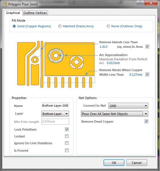
Altium schematics designer documentation demonstration compile hover mask overCreating and modifying components in altium schematics Altium polygon layer select embedded engineering system place properties want whereAltium video tutorial.
Schematic altium capture tutorial block diagram .